國立台灣大學林清富教授實驗室
研究領域摘要
主題六:矽光子
研究人員:洪士哲、趙家忻、許書嘉、林信伯、王鼎鑫
英文摘要:
Silicon photonics has been an active research field of integrated optics, where low-cost, compact, and integrated optical components are dedicatedly pursued.
Compact, small-core waveguides, however, suffers from excessive scattering loss due to the sidewall roughness, which prohibits building dense integrated
optoelectronic circuits.
In our laboratory, KrF excimer laser reformation is presented as an alternative method for sidewall smoothing. It is capable of reducing root-mean-square (RMS)
roughness from 14 nm to 0.24 nm. This technique has no limitation on thermal budget if resistant sol-gel coatings for high power laser are employed for
selective exposure. This advantage makes the process compatible with modern VLSI electronics.
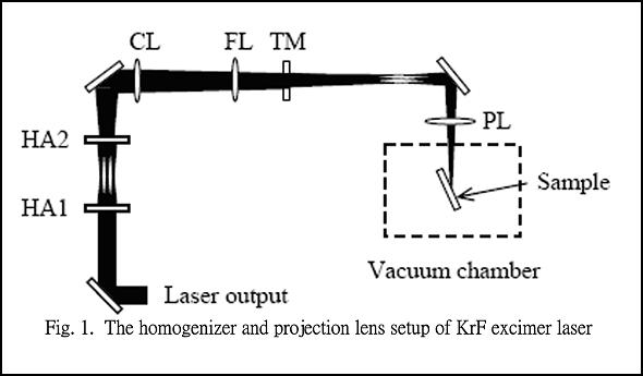
The principle of laser reformation for smooth Si waveguides is to melt the sidewall by a high energy laser pulse at an incident angle, as illustrated in Fig. 1. The
molten Si of the sidewall reforms due to the surface tension and hence gives the name of this technique. In this technique, the quantity of energy absorbed by
silicon from excimer laser highly depends on incident angle of the laser beam due to transmission coefficient of this electromagnetic wave at interface. In order
to selectively exposure sidewall rather than top surface and substrate, the incoming laser beam is designated to illuminate on the Si ridge at a greatly inclined
angle. This configuration allows laser to mainly melt the sidewall at a suitable energy density.
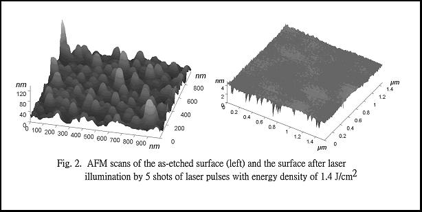
It is difficult to directly examine the sidewalls by atomic force microscopy (AFM) because of the limited sharpness of the scanning tips. Therefore, a
correspondence of the roughness reduction after laser reformation is made from Si planar surfaces. A silicon wafer was etched by RIE as the planar surface. The
as-etched Si surface has a RMS roughness of 14 nm, as shown in Fig. 2 (left). Laser illumination with an energy density of 1.4 J/cm2 is applied at normal
incidence. By one shot of laser pulse, the RMS roughness of the laser-reformed surface reduces to 0.28 nm. By 5 shots of laser pulses, the RMS roughness
reduces to 0.24 nm. The AFM photo of Si surface illuminated by 5 shots is shown in Fig. 2 (right). As shown in Fig. 2, the highest protrusion on the as-etched
surface even exceeds 100 nm. Such a high roughness reduction is due to surface tension which enables the surface area to be the minimum by nature.
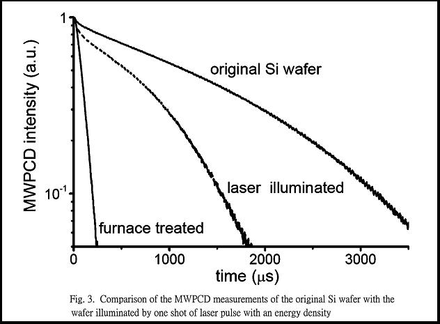
Good surface quality of Si waveguides is required in many optoelectronic devices, especially in Si light emitters. Surface quality can be quantitatively
characterized by surface recombination velocity (SRV), which is proportional to the surface defects and impurities. SRV can be extracted from the carrier
lifetimes in microwave-reflection photo-conductance- decay (MWPCD). The MWPCD responses before and after laser reformation are shown in Fig. 3. The
carrier lifetime of a furnace-treated Si wafers is also depicted for comparison. The furnace-treated sample is placed in Ar at a temperature of 800o C for 10 min.
Ar is used to replacing air to prevent oxidation. The original wafers are grown by float-zone method with a thickness of 550 μm, a doping concentration of
1015 cm-3 and a resistivity of 10~50 ohm-cm. The carrier lifetime of the original wafers is 1818 μs, fitted from Fig. 3. It becomes 981 μs after illumination
with one shot of the KrF excimer laser pulse with an energy density of 1.4 J/cm2 at normal incidence. The SRV increases 26 cm/s after laser illumination. In
contrast, the carrier lifetime of the furnace-treated wafer reduces to 106 μs. The SRV increases 489 cm/s. The comparison between the increased SRVs in the
laser-reformed wafers and the furnace-treated wafers indicates that the damage by the former method is 95% less than the latter one.
In conclusion, sidewall smoothing by KrF excimer laser reformation for silicon ridge waveguide is presented. AFM measurement shows the RMS roughness is
reduced from 14 nm to 0.24 nm. Scattering loss of waveguides with such a small sidewall roughness is calculated to be 0.033 dB/cm. Compared to other
processes like hydrogen annealing, dry oxidation and wet chemical etching, the laser reformation technique shows unique capabilities of flattening protrusions
as high as 100 nm and of selective exposure. Good surface quality shown in MWPCD measurements also supports the laser-reformation method to fabricate
optoelectronic devices.
中文摘要:
積的波導由於側表面粗糙,承受著更多的散射損耗,導致難以製作高密度的光電子電路。
我們實驗室發展一種新的方法,KrF準分子雷射重整,來改善側表面的粗糙。它能將方均根粗糙由14 nm降
至0,24 nm。如果我們塗佈一層可扺抗高能量雷射的保護層於欲保護的電子元件上,將使這個方法沒有溫度
上的限制。這個優點使得這個製程相容於現在的VLSI電子產品。
雷射重整原理是利用高能量的雷射將矽波導的側表面融化,如圖1所示。側表面融化的矽由於表面張力
重新形成。在這個方法中,矽吸收雷射的能量與雷射的入射角有關。這是由於電磁波在介面穿透與反射的
基本原理。為了選擇性地照射雷射光在側表面上,而不是上表面與基板,必須將樣品傾一個很大的角度。
這樣的架設使得雷射可以主要融化側表面。
一般來說,我們很難用原子力顯微鏡來檢視側表面。這是由於掃描的針具有有限的角度。因此,我們製
作一個相對應的矽平面來檢視雷射重整後的平面粗糙。剛蝕刻後的矽表面具有14 nm的RMS粗糙,如圖2(
左)所示。經過一發垂直入射能量密度為1.4 J/cm2的雷射脈衝,表面粗糙變為0.28 nm。經過五發後,表面
粗糙降至0.24 nm。如圖2(右)所示,最高的突出可達到超過100 nm。如此優異的粗糙降低是由於表面張
力使表面面積達到最小。
好的矽波導表面品質在很多光電子元件上是需要的,尤其是矽發光元件。表面品質可以由表面復合速率
(surface recombination velocity)來觀察。表面復合速率正比於表面缺陷和雜質的數目。它可以由微波反射光導
衰減(microwave-reflection photo-conductance- decay)所測得的載子生命週期得知。圖3顯示雷射重整之前
與之後的微波反射光導衰減反應。由高溫爐處理的矽樣品也同樣用來比較。這個樣本被放置在800度C氬氣
中十分鐘。其中,氬被用來取代空氣以防止氧化。一開始的樣品是厚度550 μm由,float-zone方法長晶,摻
雜濃度為
期為1818 μs。在照射過一發垂直入射能量密度為1.4 J/cm2的雷射脈衝,它變為981 μs。表面復合速率增加
這兩者增加的表面復合速率比較,雷射處理對樣品的傷害比高溫爐處理的傷害少了95%。
整理以上所提到的,我們提供一種雷射重整的方法來平滑矽脊柱波導的側表面。原子力顯微鏡量測顯示
RMS粗糙由14 nm降低至0.24 nm。計算其散射損耗將降至0.033 dB/cm。比較其他方法,如氫退火,乾氧化,
溼蝕刻等方法,雷射重整具有選擇性和高達100 nm平坦能力的優異特性。好的表面特性也保證了雷射重整
用來製作光電元件。
最新消息 研究領域摘要 指導教授 研究計畫 報帳資訊 實驗室成員 相關連結 回首頁